NPS-XY-100A
- 所属类别:NanoMechanisms
- 浏览次数:3938
- 发布时间:2013-07-20
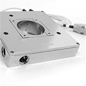
The NPS-XY-100A is a piezo scanned flexure guided stage with integrated capacitance position sensors. It is made of Super Invar and is capable of sub-nanometer resolution and reproducibility.
The NPS-XY-100A is a piezo scanned flexure guided stage with integrated capacitance position sensors. It is capable of sub-nanometer resolution and reproducibility. Finite element analysis of the flexure guidance mechanisms has reduced parasitic angular motions to less than 25 micro-radians over the full 100 micron range.
The Super Invar construction (CTE 0.3ppm K-1, c.f. Al at 23ppm K-1) minimizes thermal drift, which on a nanometer scale is very important. The unique isostatic mounting system ensures that stresses from the mounting system are properly relieved and establishes the center of the stage as the co-ordinate reference point.
Features
- > 100 micrometer travel in each axis with sub-nanometer resolution
- < 0.005% hysteresis and linearity error
- First resonant frequency > 350 Hz
- High bandwidths (> 50 Hz) and fast response times
- In-situ scanning and stepping response optimization
- Use with NPS-Z-15A or NPS-Z-15H for XYZ options
- Super Invar construction
Applications
- High Precision Microscopy
- AFM, SPM, NSOM
- Suggested Controller
- NPS3220
Related Products
- NPS-XY-100B (aluminium)
 类别
类别